
The Intel Foundry Technology Research team today announced technological breakthroughs in 2D transistor technology using non-silicon materials, chip-to-chip interconnects and packaging technology, among others. The company will present the results of its research in seven papers of its own and in two further papers produced in collaboration with industry partners such as imec at the IEEE International Electron Devices Meeting (IEDM) 2024.
Intel’s disclosures include recent research that improves the scaling and performance of Gate-all-Around (GAA) transistors on both silicon and atomically lean 2D transistors using materials other than silicon. Intel also introduced its subtractive ruthenium technology, which improves interconnect performance and scalability by enabling smaller wires between transistors, and a breakthrough chip packaging solution that increases chip-to-chip assembly throughput 100-fold.
The Intel Technology Research Team, previously known as the Component Research Team for the past 50 years, is part of the Intel Foundry. This team works to develop products intended for commercialization in the near term rather than the more far-reaching initiatives at Intel Labs. The technology research team is known for paving the way for many of Intel’s core technologies, introducing the latest innovations such as PowerVia rear power and the versatile RibbonFET architecture with a RibbonFET gate derived from this group.
Intel has not yet presented documents at IEDM, and our one-on-one discussion with the research team’s CEO will not take place until tomorrow. We’ll provide breakdowns of the breakthroughs below, but we’ll be back with an update to provide more details.
A breakthrough in scaling interconnections
As transistors get smaller, so do the wires (connectors) that connect them. Copper is the material of choice for the billions of nanometer-scale wires that transmit power and data inside the chip in a sophisticated 3D grid (you can see what it looks like in this video). In fact, contemporary chips contain up to 50 miles of interconnect cabling. However, the shrinkage capacity of these microscopic wires is exhausted, and most alternatives are not suitable for large-scale production. This is a critical obstacle to moving to smaller process nodes.
Like the standard copper wire used in your home to connect electrical devices, the wires that carry electrons between transistors require an insulator, in this case a dielectric coating, to prevent electrons from going where they shouldn’t. However, the cables also require a barrier to prevent the diffusion of copper, which could contaminate the dielectric. This barrier causes problems with tubing shrinkage.
Shrinking interconnect wires in a processor is extremely tough due to the requirements of Damascus copper, the additive process used to create the wires. First, a trench is created, then a barrier is placed on the dielectric in the trench. A seed layer is then placed on top of the barrier to allow for copper electroplating; then copper settles on top. The excess material at the top is then polished.
As shown in the image above, reducing the amount of copper helps dilute the wire, but it also reduces the ratio of copper (mass) to the barrier and starting layers, and the resistivity increases exponentially as the wires shrink. This means the wires carry less current, which slows down the speed of the device (among other things) and affects capacity.
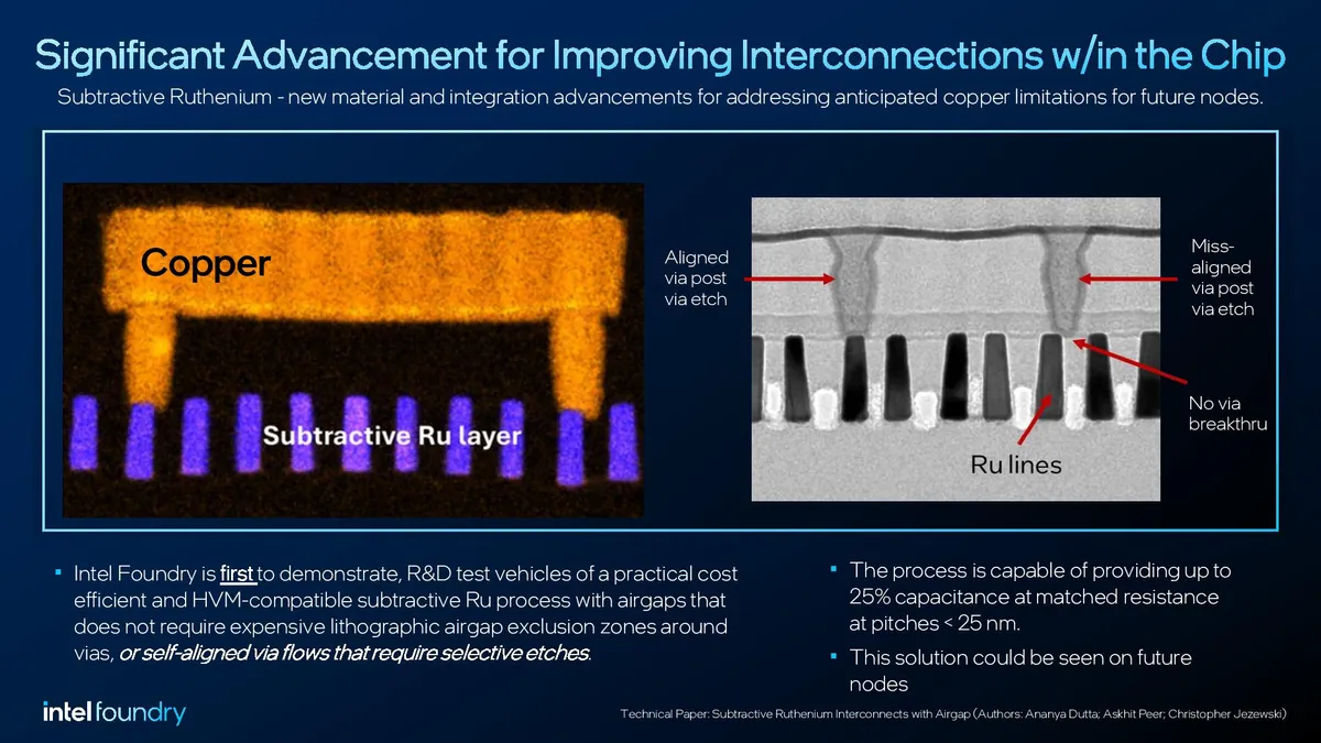
Intel’s technology research team has developed a process suitable for large-scale production that uses ruthenium instead of copper. It also has air gaps.
Air gaps are a technology that Intel introduced on the 14nm process node. This technique removes sections of the insulating dielectric, leaving air instead (air has a dielectric constant of about 1.0) to reduce capacity (Intel claimed capacity increased by 17% at 14nm).
Intel hasn’t shared specific details of the subtractive ruthenium process, but we’ll certainly learn more details during the presentation. Intel claims its subtractive ruthenium air-gap process delivers up to 25% capacity with matched resistance at pitches of less than 25nm (center-to-center distance between interlines). Intel says its research team is “the first to demonstrate in R&D test vehicles a practical, cost-effective, and mass-production-compatible integrated air-gapped subtractive Ru process that does not require costly lithographic air-gap exclusion zones around vias or self-alignment through flows requiring selective digestion.”

Intel anticipates using this technique first for the most critical layers with the smallest gaps, while standard Damascus copper will be used for the larger upper layers. Naturally, Rutheniuem will also be beneficial for PowerVia rear power. Ultimately, these smaller wires will enable the connection of smaller transistors, and Intel says this technology will likely be used in future Intel Foundry nodes.
A breakthrough in the field of Gate-All-Around (GAA) transistors.
Picture 1 With 3


Intel’s RibbonFET is the first recent transistor design since the advent of FinFET over 13 years ago. This is Intel’s first Gate-all-Around (GAA) transistor, debuting with 20A and 18A nodes. It features stacked nanosheets completely surrounded by a gate, unlike the three-sided fins used in FinFETs.
Picture 1 With 3


The challenge now is to further shrink GAA designs, and Intel is trying to address this with both standard silicon designs and new 2D materials. On standard silicon, Intel’s unveiled transistors demonstrate improved scaling of the entire RibbonFET CMOS gate, resulting in a 6nm gate length and a 1.7nm nanoribbon/nanosheet thickness, while providing improved short-channel effects and higher performance.
First, the gate length versus electron velocity plot on the right shows an impressive profile. The table in the center of the slide shows comparisons to existing transistor technologies, with the Tfin/Tsi (fin thickness/nanotube thickness) for the nanoribbon being almost twice thinner than the fin used in FinFET.
The big question is: what’s next after silicon? With the advent of CFET transistors, GAA’s next step is to change the materials used in NMOS and PMOS transistors to 2D materials (only a few atoms thick). The second slide shows Intel’s progress in the use of atomically thin transition metal dichalcogenide (TMD) materials, commonly considered the post-silicon materials.
Intel has produced versatile 2D gate NMOS and PMOS transistors with a gate length of 30 nm using a mole-based material. Intel claims these efforts resulted in “best-in-class NMOS drive currents,” which is a two-fold improvement over the next best published result. The graph on the right shows that the research vehicle is outperforming other such TMD research efforts.
Intel’s transistor list also includes a look back at the last 60 years of transistor technology and a call to action for the industry to develop transistors that operate at ultra-low Vdd supply voltages of less than 300 mV, a significant drop from today’s 1 V range. This is a goal stretched into the 1930s and 1940s.
Breakthroughs in packaging

Intel’s new Selective Layer Transfer Technology (SLT) enables an entire chip board to be connected to another board at extremely high speeds – Intel says SLT enables a 100-fold increase in throughput in the chip-to-chip assembly process. With SLT, an entire board full of dies can be connected to the board underneath at once, and individual dies can be selected for bonding and others can be excluded. This technology uses inorganic infrared laser peeling.
Intel also cites that SLT “enables ultra-thin chiplets with significantly greater flexibility, allowing for smaller die sizes and higher form factors compared to conventional chip-to-wafer assembly.” Intel’s descriptions of this new technology aren’t entirely clear, so we hope to learn more from the presentation. This seems like it would be a great alternative to approaches using reconstituted wafers. As we learn more, we will add more details here.

Intel will also deliver a lecture on future packaging solutions, invited by IEDM. The slide above revealed EMIB-T, which has not been disclosed before. As a reminder, EMIB is Intel’s built-in Multi-Die Interconnect Bridge, a low-latency, low-power, high-bandwidth interconnect that connects modules together.
Intel revealed that EMIB-T stands for EMIB-TSV. This variant is the first EMIB implementation that uses TSV to transmit the signal across the bridge using the TSV instead of wrapping the signal around the bridge.
Picture 1 With 4


At IEDM, Intel will present seven papers and two other papers with partners such as imec, Aixtron and Tor Vergata University of Rome.
We have time with Intel for further questions and will update this article with more details soon.